


fgonz031
Well-known member
- Joined
- Mar 11, 2024
- Messages
- 59
- Reaction score
- 18
- Points
- 8
JP 2026-119574 A proposes a pixel-level charge-bleeding CMOS image sensor that uses a controllable constant-current path across the photodiode to prevent saturation, extend dynamic range, and emulate an electronic ND filter without physically reducing incoming light.
What it does
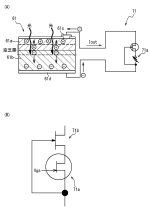
Each pixel includes a photodiode plus a constant-current discharge circuit that removes charge during exposure at a known rate.
The sensor reconstructs the total collected charge as “stored charge + discharged charge,” so highlight information can be recovered even when the photodiode would otherwise saturate.
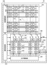
The discharge current is programmable, typically via an FET-based variable resistor and a DAC-controlled bias, enabling per-pixel or per-block tuning.
The same mechanism can be used to simulate an optical ND filter electronically, including frame-to-frame adaptation for video.
Why it matters
It targets a real bottleneck in CMOS sensors: loss of highlight detail due to photodiode saturation.
Unlike a physical ND filter, it preserves full photon arrival at the sensor, which helps low-light SNR while still controlling exposure-like behavior digitally.
The architecture is especially relevant for cinema, HDR imaging, surveillance, and automotive systems that face rapidly changing brightness.
Key technical strengths
Maintains linearity while extending effective dynamic range.
Avoids mechanical or optical ND components.
Supports adaptive exposure control using pre-exposure or previous-frame statistics.
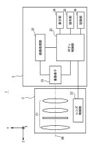
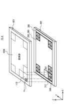
Can be implemented in a stacked-sensor architecture, with pixel array on one die and control/processing on another.
Main limitations and risks
Adds analog complexity, calibration burden, and pixel-area overhead.
Per-pixel current control may be sensitive to process, temperature, and mismatch variation.
The approach depends on accurate reconstruction of the discharged charge; if control drifts, image error or FPN can increase.
Global shutter
Yes of course— it mentions global shutter, but only as an optional modification, not as the core invention.
The patent says that “for global electronic shutter operation, a charge-holding section may be provided between the transfer part 62 and the floating diffusion 63,” which is essentially a side note about a possible implementation. However, the claims and the main embodiments do not define a global-shutter pixel architecture, storage node, or simultaneous exposure/readout sequence.
So the accurate reading is: global shutter is referenced, but not disclosed as the main operative mode or claimed novelty. The invention’s real focus is the constant-current charge release / HDR / electronic ND mechanism.
Patent scope in one line
The core claim is not “better HDR” in general, but a specific photodiode-connected constant-current release circuit whose known discharge is used to both suppress saturation and mathematically recover the lost charge.
Strategic take
For sensor companies, this reads like a platform patent for smart pixels: wide DR, electronic ND, and possibly per-region exposure shaping from the same circuit block. If you want, I can turn this into a more formal one-page executive brief with sections like novelty, claim scope, FTO risk, and competitive impact.
JP 2026-119574 JPLATPAT
What it does
Each pixel includes a photodiode plus a constant-current discharge circuit that removes charge during exposure at a known rate.
The sensor reconstructs the total collected charge as “stored charge + discharged charge,” so highlight information can be recovered even when the photodiode would otherwise saturate.
The discharge current is programmable, typically via an FET-based variable resistor and a DAC-controlled bias, enabling per-pixel or per-block tuning.
The same mechanism can be used to simulate an optical ND filter electronically, including frame-to-frame adaptation for video.
Why it matters
It targets a real bottleneck in CMOS sensors: loss of highlight detail due to photodiode saturation.
Unlike a physical ND filter, it preserves full photon arrival at the sensor, which helps low-light SNR while still controlling exposure-like behavior digitally.
The architecture is especially relevant for cinema, HDR imaging, surveillance, and automotive systems that face rapidly changing brightness.
Key technical strengths
Maintains linearity while extending effective dynamic range.
Avoids mechanical or optical ND components.
Supports adaptive exposure control using pre-exposure or previous-frame statistics.
Can be implemented in a stacked-sensor architecture, with pixel array on one die and control/processing on another.
Main limitations and risks
Adds analog complexity, calibration burden, and pixel-area overhead.
Per-pixel current control may be sensitive to process, temperature, and mismatch variation.
The approach depends on accurate reconstruction of the discharged charge; if control drifts, image error or FPN can increase.
Global shutter
Yes of course— it mentions global shutter, but only as an optional modification, not as the core invention.
The patent says that “for global electronic shutter operation, a charge-holding section may be provided between the transfer part 62 and the floating diffusion 63,” which is essentially a side note about a possible implementation. However, the claims and the main embodiments do not define a global-shutter pixel architecture, storage node, or simultaneous exposure/readout sequence.
So the accurate reading is: global shutter is referenced, but not disclosed as the main operative mode or claimed novelty. The invention’s real focus is the constant-current charge release / HDR / electronic ND mechanism.
Patent scope in one line
The core claim is not “better HDR” in general, but a specific photodiode-connected constant-current release circuit whose known discharge is used to both suppress saturation and mathematically recover the lost charge.
Strategic take
For sensor companies, this reads like a platform patent for smart pixels: wide DR, electronic ND, and possibly per-region exposure shaping from the same circuit block. If you want, I can turn this into a more formal one-page executive brief with sections like novelty, claim scope, FTO risk, and competitive impact.
JP 2026-119574 JPLATPAT
Attachments
-
 JPA 508119574_i_000002.jpg89.3 KB · Views: 0
 -
 JPA 508119574_i_000005.jpg96.4 KB · Views: 0
 -
 JPA 508119574_i_000006.jpg117.4 KB · Views: 1
 -
 JPA 508119574_i_000003.jpg107.3 KB · Views: 1
 -
 JPA 508119574_i_000013.jpg144.9 KB · Views: 1
 -
 JPA 508119574_i_000004.jpg291.9 KB · Views: 0
 -
 JPA 508119574_i_000012.jpg344.6 KB · Views: 0